IDE: Renesas e² studio Ver 2020-10 (20.10.0).
CCRX Compiler Version: 3.02.00
Target Processor: RX651 (R5F5651CDDBG) on custom board
Segger Software Installed: J-Link V6.88C package
Segger Tool: Jlink Ultra +
Hello,
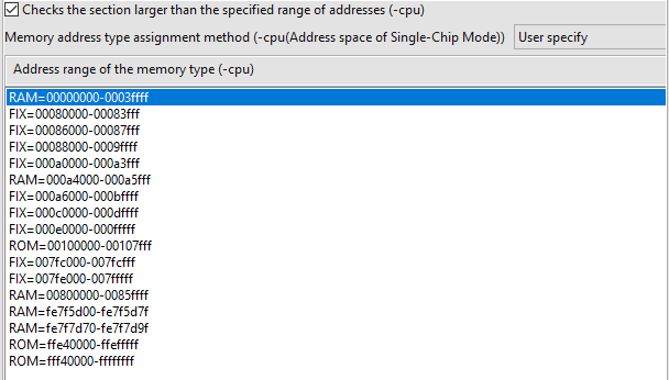
I am currently developing code on the Renesas RX651 processor and I am using Jlink Ultra+ to debug my custom board. I have my RX651 configured as dual bank flash mode. When having the chip configured this way, the valid address range we get for our code flash is 0xFFE40000 – 0xFFEFFFFF for bank 1 and 0xFFF40000 – 0xFFFFFFFF for bank 0, giving us a total of 1.5Mbytes combined. When the chip is setup as linear mode, valid address range we get for our code flash is 0xFFE80000 – 0xFFFFFFFF which is also 1.5Mbytes. The issue I was running into is that Jlink doesn’t seem to support the Dual bank memory layout for my chip. I get this warning (See Image JlinkDebugWarning.png) message when I am debugging from E2Studio using Jlink.

I know what the warning is but the Jlink doesn’t have R5F5651CDxBG_DUAL selection so I used the only one that was available, R5F5651C when setting up the Jlink with the Debugger. When ignoring this warning and clicking yes, as expected, I get the following error (See Image jlinkWriteError.png ) when writing data anywhere in 0xFFE40000-0xFFE7FFFF.

I verified that no Data was written in locations 0xFFE40000-0xFFE7FFFF by the Jlink. From here I assumed that the Jlink is using a linear mode, and it is assuming that I am trying to write to a reserved location. So, my question is:

All suggestions are welcome. Thanks in advance
CCRX Compiler Version: 3.02.00
Target Processor: RX651 (R5F5651CDDBG) on custom board
Segger Software Installed: J-Link V6.88C package
Segger Tool: Jlink Ultra +
Hello,
I am currently developing code on the Renesas RX651 processor and I am using Jlink Ultra+ to debug my custom board. I have my RX651 configured as dual bank flash mode. When having the chip configured this way, the valid address range we get for our code flash is 0xFFE40000 – 0xFFEFFFFF for bank 1 and 0xFFF40000 – 0xFFFFFFFF for bank 0, giving us a total of 1.5Mbytes combined. When the chip is setup as linear mode, valid address range we get for our code flash is 0xFFE80000 – 0xFFFFFFFF which is also 1.5Mbytes. The issue I was running into is that Jlink doesn’t seem to support the Dual bank memory layout for my chip. I get this warning (See Image JlinkDebugWarning.png) message when I am debugging from E2Studio using Jlink.
I know what the warning is but the Jlink doesn’t have R5F5651CDxBG_DUAL selection so I used the only one that was available, R5F5651C when setting up the Jlink with the Debugger. When ignoring this warning and clicking yes, as expected, I get the following error (See Image jlinkWriteError.png ) when writing data anywhere in 0xFFE40000-0xFFE7FFFF.
I verified that no Data was written in locations 0xFFE40000-0xFFE7FFFF by the Jlink. From here I assumed that the Jlink is using a linear mode, and it is assuming that I am trying to write to a reserved location. So, my question is:
- How do I make Jlink support dual memory mode for my Chip?
- How do I tell E2Studio to use a different Jlink dll or update the Jlink dll that comes pre-installed with E2Studio? (For example, if I want to use the Jlink DLL that gets installed with J-Link V6.88C package instead of the one that is provided by E2Studio)
- Any workarounds you can suggest?
All suggestions are welcome. Thanks in advance


