


Hi everyone,
I am using the J-Link plus compact, and I am facing an issue regarding the reference voltage. The probe does not read the correct reference voltage and I cannot flash my boards because of a low reference voltage.
I have designed a custom PCB that integrates the nRF52840 SOC. I use the SWD interface to communicate the probe with the SOC and the system’s voltage is 1.8V.
The setup
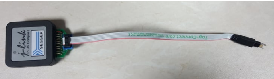
I use a 20 to 6 pin adapter and a 6 Pin plug of nailto hardware connect the J-link with the PCB
Measurements
I have measured the VTref at both the PCB and the J-Link connector and I confirm that I read 1.8V. So, I am sure that I provide 1.8V as the target reference voltage to the J-Link.
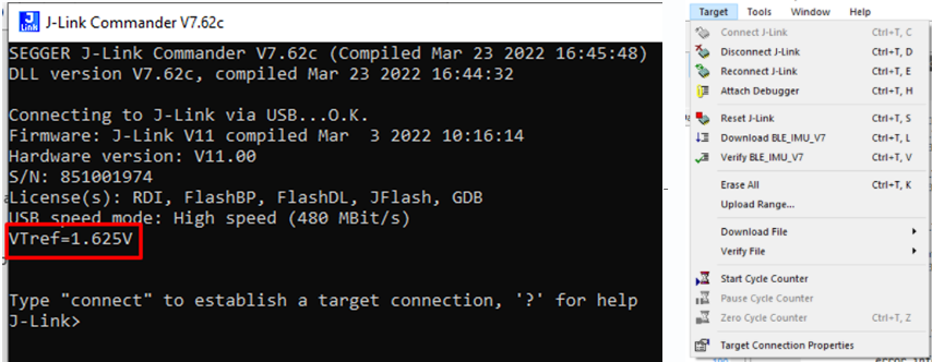
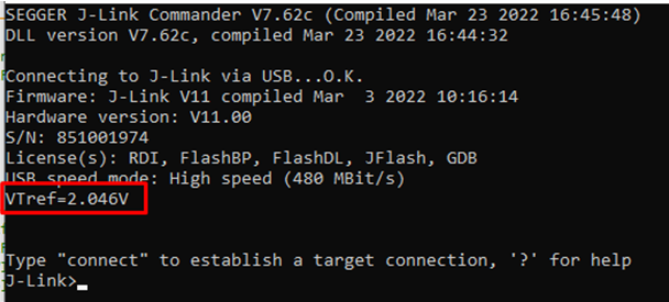
However, when I run the J-Link commander the reference voltage varies. I have measured three cases and the VTref varies from 1.451 - 2.046V. However, when I measure with the multimeter I measure 1.8V for each case:
No connection of J-Link with the target (from SES)

Connection of J-Link with target (from SES)
When enter the debug mode from SES
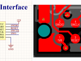
Just for reference, this is my PCB schematic and layout for SWD interface
I am using the J-Link plus compact, and I am facing an issue regarding the reference voltage. The probe does not read the correct reference voltage and I cannot flash my boards because of a low reference voltage.
I have designed a custom PCB that integrates the nRF52840 SOC. I use the SWD interface to communicate the probe with the SOC and the system’s voltage is 1.8V.
The setup
I use a 20 to 6 pin adapter and a 6 Pin plug of nailto hardware connect the J-link with the PCB
Measurements
I have measured the VTref at both the PCB and the J-Link connector and I confirm that I read 1.8V. So, I am sure that I provide 1.8V as the target reference voltage to the J-Link.
However, when I run the J-Link commander the reference voltage varies. I have measured three cases and the VTref varies from 1.451 - 2.046V. However, when I measure with the multimeter I measure 1.8V for each case:
No connection of J-Link with the target (from SES)
Connection of J-Link with target (from SES)
When enter the debug mode from SES
Just for reference, this is my PCB schematic and layout for SWD interface